The manufacturing process of a PCB (Printed Circuit Board) is an assembly line involving multiple steps, which can be broadly categorized into the following stages. It’s important to note that different board structures may entail distinct processes; the following workflow outlines the comprehensive fabrication process for multi-layer PCBs.
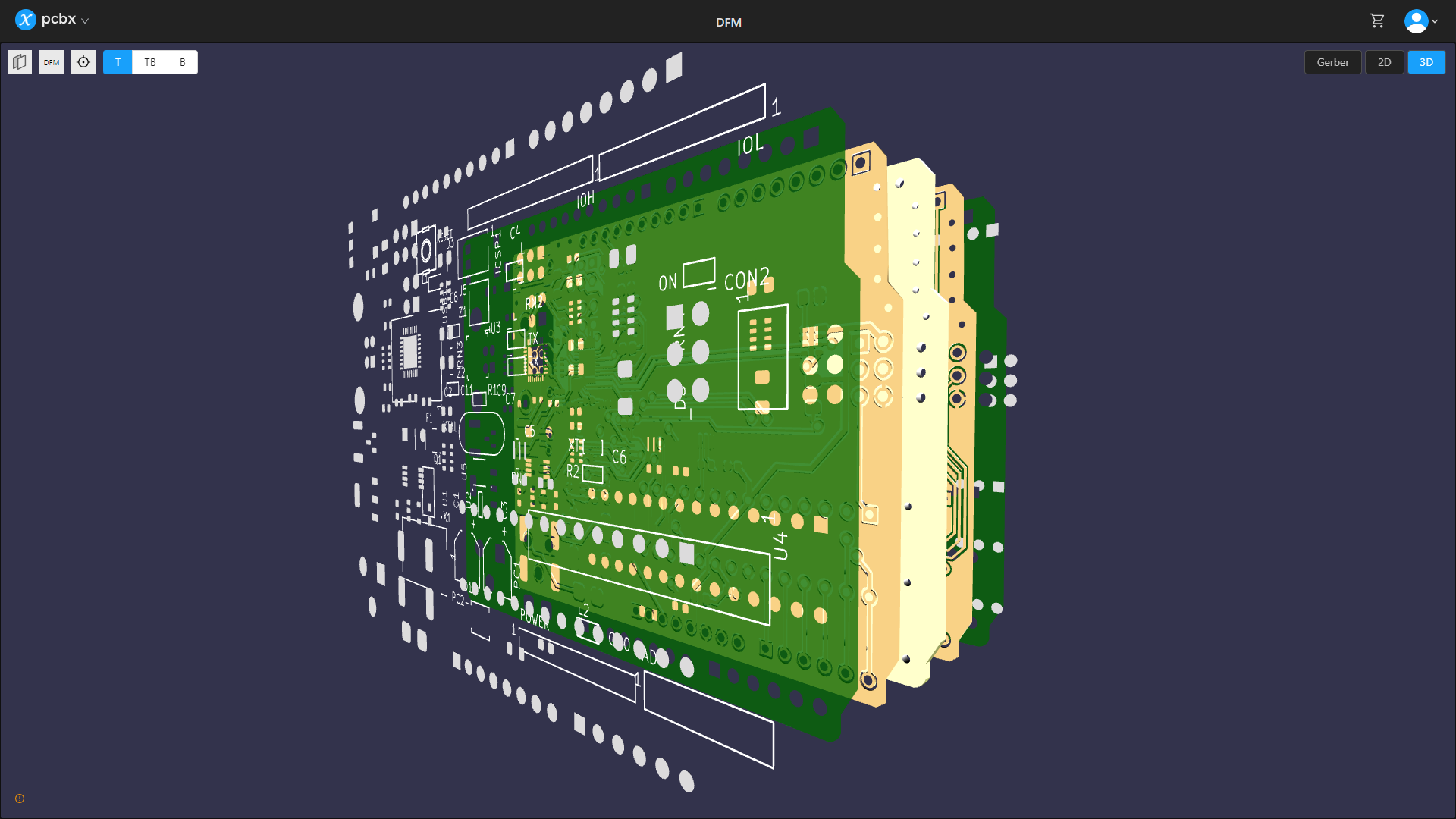
- Files & DFM: Acquiring production-ready files.
-
- PCB Layout: Creating a PCB layout using specialized CAD software and exporting engineering files.
- Conversion to Gerber: Transferring engineering files into Gerber format.
- DFM (Design for Manufacturing): Examining the manufacturability and reliability of the PCB layout through the Gerber file.

- Inner Layer Transfer: Fabricating the inner layer circuits of the PCB.
- Laminating: Forming a negative image on the copper-clad laminate based on design files using photolithography or digital imaging techniques.
- Pre-treatment: Cleaning and activating the surface of the laminate to ensure good adhesion of the resist.
- Dry Film/Wet Film Application: Applying a photosensitive film onto the copper surface of the laminate to protect non-circuit areas from etching.
- Exposure: Using exposure equipment with UV light passing through a mask containing circuit pattern information to harden the film in exposed areas; unexposed parts dissolve during development.
- Development: Removing the dry film/wet film from unexposed areas, revealing the copper layer to be etched.
- Etching: Utilizing chemical solvents to remove the unprotected copper, forming the desired circuit pattern.
- Stripping and Post-processing: After etching, removing the cured dry film and conducting post-processing steps like cleaning, microetching to optimize copper surface quality.

- Inner Layer Inspection: Detecting and repairing inner layer circuits.
-
- AOI (Automated Optical Inspection): Scanning the inner layers with optical devices to check if they meet design requirements and identify any broken lines, short circuits, etc.
- Repair: Conducting repairs such as patching or other necessary work to ensure circuit integrity where issues are detected.
- Lamination: Bonding multiple layers into a single board.
- Preginning: Performing pre-treatment on the etched inner copper layers to form a layer of copper oxide, enhancing interlayer bonding strength and increasing the roughness of the copper surface.
4. Lamination Preparation: Cutting appropriate prepregs and preparing copper foil layers of corresponding dimensions.
-
- Layer Stacking: Sequentially placing inner layers, prepregs, and copper foils in a stack and securing their positions.
- Pressing: Placing the stack into a laminating machine (e.g., a vacuum hot press), where resin melts and diffuses, firmly bonding all layers together.

5. Drilling: Creating vias for inter-layer conductivity.
-
- Drilling: Using drilling machines to create through-hole vias in the board, connecting separate copper layers for subsequent component insertion and improving heat dissipation properties.
- Post-processing: Cleaning and de-burring the board after drilling.
6. PTH: Achieving inter-layer conductivity via electroless plating or electroplating, while also increasing copper thickness.

- Outer Layer Transfer: A process similar to the inner layers.
- Pre-treatment: Acid washing, brushing, and drying the board surface to enhance dry film adhesion.
- Dry Film/Wet Film Application: Coating the outer copper foil with dry film/wet film.
- Exposure: Using a photomask to transfer the circuit pattern onto the resist, leaving hardened resist only on the intended circuit paths.
- Development: Washing away unexposed resist, leaving hardened resist only over the designated circuit locations.
- Copper Plating: Depositing copper only on the areas protected by the resist, forming the outer layer circuit pattern.
- Outer Layer Etching: Finalizing the multi-layer PCB layout.
- Etching: Using strong alkali solutions to remove excess copper foil not covered by the resist.
- Resist Removal: Clearing away the resist that has completed its protective function.
- Desmear: Removing tin plating from the PCB layout copper foil using a desmear solution.
- Solder Mask: Protecting copper circuits from oxidation.
- Pre-treatment: Acid washing and ultrasonic water cleaning to remove board oxides and increase copper surface roughness.
- Printing: Covering areas of the PCB not requiring soldering with solder mask ink, providing insulation and protection.
- Pre-baking: Drying solvent in the solder mask ink and partially hardening it for exposure.
- Exposure: Curing the solder mask ink.
- Development: Removing uncured sodium carbonate solution from the non-polymerized solder mask.
- Post-bake: Fully hardening the solder mask ink.
- Screen Printing: Adding identification marks and text to the board.
- Acid Wash: Cleaning the board surface to remove oxidation, enhancing adhesion of printing ink.
- Printing: Imprinting model numbers, orientation indicators, and other information on the board surface.
- Surface Finish: May include various surface finishing methods such as gold plating, HASL (Hot Air Solder Leveling), ENIG (Electroless Nickel Immersion Gold), OSP (Organic Solderability Preservative) to enhance solderability and corrosion resistance of pads and conductive areas.
- Electrical Testing: Rigorously testing the PCB electrically by probing test points to verify correct connections between circuit segments and detecting potential shorts or opens that could lead to board failure.
- Cutting or Routing: Trim the final PCB outline according to the designed dimensions and shape.
- FQC/OQC: Conducting sampling inspections after all processes, visually or using AOI machines, to check for physical defects and ensure compliance with stringent industry standards and any customer-specific requirements.
- Packaging & Shipping: Vacuum packaging the PCBs to protect them from static, impact, moisture, etc., during transportation, then sending them to the customer.
Leave A Comment