Title: An Introduction to PCBs: From Design to Assembly
Introduction:
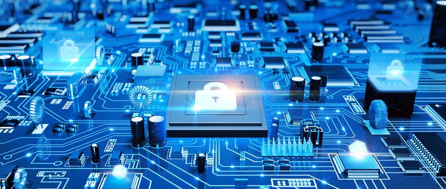
Printed Circuit Boards (PCBs) are the fundamental building blocks of most electronic devices. They serve as a platform for mounting and interconnecting electronic components, thereby facilitating signal transmission and power distribution in a highly organized and efficient manner. This article aims to provide a comprehensive overview of what PCBs are, the stages involved in their design, manufacturing process, and assembly.
- What is a PCB?
A PCB is a non-conductive substrate, typically made from materials like fiberglass, epoxy resin, or other composite materials, which has conductive pathways or traces etched onto it. These pathways allow electrical signals and power to flow between different electronic components mounted on the board. The components are attached using soldering, while vias and through-holes connect circuits on multiple layers. PCBs come in various forms, ranging from single-layer boards used in simple devices to complex multilayer ones found in high-end electronics.
Typically, a PCB consists of multiple layers:
- Substrate: The base material which gives the PCB its rigidity.
- Copper Layer: Thin sheet(s) of copper foil laminated to the board, providing conductive paths.
- Solder Mask: A protective layer that prevents short circuits and protects the copper from the environment.
- Silkscreen: Printed labels on the PCB to indicate component locations, test points, or other markings.

- PCB Design
The design of a PCB starts with a schematic diagram, representing the electrical components and their connections. This theoretical circuit map is then translated into a PCB layout using Computer-Aided Design (CAD) software. The layout specifies the precise placement of components and the routing of traces (conductive paths) that connect these components.
The design of a PCB must consider many factors:
- Electrical properties: Including resistance, capacitance, and inductance of the traces.
- Mechanical constraints: The size and shape of the PCB must fit within the product.
- Heat management: Heat dissipation pathways are essential for maintaining component functionality.
- Electromagnetic compatibility: Designs must minimize electromagnetic interference to ensure stable operation.
III. PCB Manufacturing
The manufacturing of PCBs is a complex multistep process that requires precision and attention to detail. Here’s an overview of the key stages:
- Design: Using specialized software like Altium Designer or Cadence, engineers design the PCB, creating a circuit schematic, component layout, and routing.
- Photolithography: The design is transferred to a photosensitive film, which is then exposed to light and developed to create a negative image of the circuit.
- Etching: The copper is etched with a chemical solution to remove the unwanted parts and leave behind the circuitry.
- Drilling: Holes are drilled into the PCB for component leads and for through-hole connectors.
- Plating: The board is plated to prevent oxidation and improve conductivity and solderability.
- Assembly: Components are attached to the PCB, either through-hole or surface mount, depending on the design.
- Testing: The PCB is tested to ensure that the circuit functions correctly.
- PCB Assembly
The final phase is the assembly, where components are soldered onto the board. There are two primary methods:
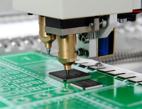
- a) Surface Mount Technology (SMT): Components are placed directly onto the surface of the PCB pads, often with the aid of a pick-and-place machine. Solder paste, previously screen-printed onto the board, melts during reflow soldering, securing the components in place.
- b) Through-Hole Technology (THT): Components with leads are inserted through holes in the board, then secured on the opposite side by wave soldering or manual soldering.
Post-assembly, the PCB undergoes rigorous inspections and tests, including Automated Optical Inspection (AOI), X-ray inspection for hidden joints, In-Circuit Tests (ICT), and functional tests to ensure quality and functionality.
Conclusion:
PCBs remain integral to electronic design and innovation. They have come a long way from their origins but maintain their status as the essential enablers of electronic functionality. As technology evolves, so too will PCBs, adapting to facilitate the ever-growing demands of new and improved devices. Understanding the complexity and importance of PCBs offers insight into the silent workhorse that powers the modern world’s electronic marvelries.
Leave A Comment