Introduction:
Printed Circuit Board (PCB) assembly is a complex and intricate process that involves transforming a bare board into a fully functional electronic device. This detailed article aims to provide a comprehensive overview of the different stages involved in PCB assembly. The process, also known as Printed Circuit Board Population or PCBA, integrates numerous electronic components onto a PCB to create a unified circuit capable of performing specific functions.
Step 1: Solder Paste Stenciling
The first stage in PCB assembly is the application of solder paste. Just like an artist applying paint to a canvas, the stencil, a thin sheet with apertures cut into it, helps apply solder paste to the specific areas where components will be placed. It’s vital that only the right places receive solder paste, which is a mixture of fine solder particles and a sticky flux. A squeegee blade moves across the stencil, pushing the solder paste through the open areas and onto the PCB. This step sets the stage for making strong solder joints between the PCB surface and the electronic components.
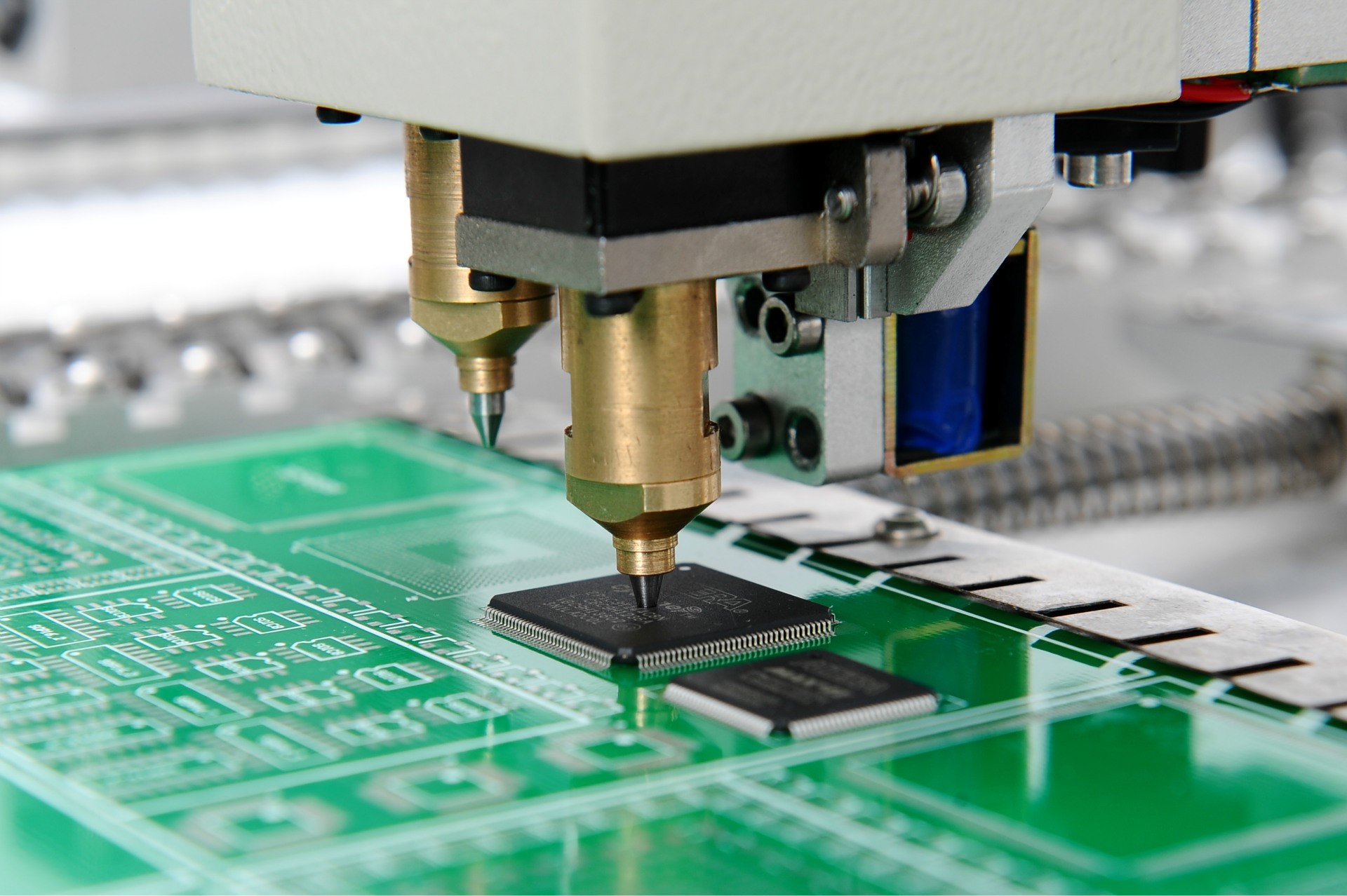
Step 2: Pick and Place
After the application of solder paste, components need to be placed on the board accurately. High-speed robotic machines, aptly named pick-and-place machines, rapidly and precisely place surface-mount devices (SMDs) onto the solder-pasted PCB. Each component is picked up from a reel or feeder by a vacuum nozzle on the machine and then placed on the designated solder pad on the board. Industrial pick-and-place machinery rapidly accelerates this process, allowing for the assembly of thousands of components per hour with extraordinary accuracy.

Step 3: Soldering
With all components on their assigned pads, the PCB now heads to the soldering equipment. There are different soldering techniques, but the most common one for SMDs is reflow soldering. The populated PCB is conveyed into a reflow soldering oven wherein controlled heat is applied. The temperature increases gradually to prevent component damage and to allow the flux in the solder paste to clean and prepare the metal surfaces. The board reaches a peak temperature that melts the solder, effectively making electrical connections between components and the board. As the PCB then cools, the solder solidifies and forms strong electrical and mechanical bonds.
For through-hole components, wave soldering is a commonly used technique. The PCB, with pins protruding through, passes over a wave of molten solder that wets the exposed metal areas and creates a joint. In some cases, especially when dealing with complex boards or sensitive components, manual soldering by technicians might be necessary.
Step 4: Inspection and Quality Control
It’s critical to ensure that all the solder joints are perfect and that there are no errors such as misaligned components or solder bridges between adjacent contacts. Inspection can be done visually by skilled technicians or via automated methods, such as Automated Optical Inspection (AOI). AOI machines use high-resolution cameras to scrutinize the PCBs for any assembly defects or anomalies. More advanced methods like Automated X-ray Inspection (AXI) are used to check for hidden issues, such as problems inside the PCB layers or under the components.
Step 5: Testing
Once the PCB assembly passes inspection, it’s subjected to various tests to validate its functionality. Some common tests include:
– In-Circuit Testing (ICT): Probes check individual components for correct placement and functionality.
– Functional Testing: The PCB is powered on, and its functional performance is compared to the design specifications.
– Burn-In Testing: The board is operated under stressful conditions for an extended period to ensure reliability.
Step 6: Through-Hole Component Insertion (if applicable)
If the PCB design includes through-hole components, these parts usually can’t be placed by standard pick-and-place machines and often require separate insertion either by hand or with specialized automation, depending on volume and component type.
Step 7: Final Inspection
A final round of inspections is done to ensure no new issues have been introduced during the soldering or testing phases. This might involve another pass through AOI or a manual check by a technician.
Step 8: Washing
Flux residue from soldering can be corrosive or conductive, and as such, it’s important to clean it off the PCB after soldering is completed. The boards may be washed with deionized water or solvents, and they are often dried to remove any remaining moisture.
Step 9: Conformal Coating
In certain applications where the PCB will be exposed to harsh environments, a conformal coating is applied to protect the board from moisture, dust, chemicals, and temperature extremes. The coating is typically a thin layer of acrylic, silicone, or urethane material that ‘conforms’ to the contours of the PCB, sealing in the components and protecting them.
Step 10: Final Assembly
Some PCBs require additional hardware, like heatsinks, cases, or connector blocks before they can be shipped. This stage may also include programming of microcontrollers or other firmware on the PCB.
Step 11: Packaging and Shipping
Finally, the completed PCBs are carefully packaged to shield them from electrostatic discharge, damage, and environmental factors. Then,, they are ready to be shipped out to their final destinations, where they will be integrated into larger systems or products.
Leave A Comment